
Access the latest CBSE Class 12 Physics Semiconductor Materials Device And Simple Worksheet. We have provided free printable Class 12 Physics worksheets in PDF format, specifically designed for Chapter 14 Semiconductor Electronics Materials Devices and Simple Circuits. These practice sets are prepared by expert teachers following the 2025-26 syllabus and exam patterns issued by CBSE, NCERT, and KVS.
Chapter 14 Semiconductor Electronics Materials Devices and Simple Circuits Physics Practice Worksheet for Class 12
Students should use these Class 12 Physics chapter-wise worksheets for daily practice to improve their conceptual understanding. This detailed test papers include important questions and solutions for Chapter 14 Semiconductor Electronics Materials Devices and Simple Circuits, to help you prepare for school tests and final examination. Regular practice of these Class 12 Physics questions will help improve your problem-solving speed and exam accuracy for the 2026 session.
Download Class 12 Physics Chapter 14 Semiconductor Electronics Materials Devices and Simple Circuits Worksheet PDF
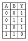
Question. In the following circuit, the output Y for all possible inputs A and B is expressed by the truth table.
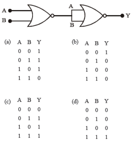
Answer: C
Question. What is the voltage gain in a common emitter amplifier, where input resistance is 3 Ω and load resistance 24 Ω, β = 0.6 ?
(a) 8 . 4
(b) 4 . 8
(c) 2 . 4
(d) 480
Answer: B
Question. In a common emitter transistor amplifier β = 60, Ro = 5000 Ω and internal resistance of a transistor is 500 Ω. The voltage amplification of amplifier will be
(a) 500
(b) 460
(c) 600
(d) 560
Answer: C
Question. The band gap in germanium and silicon in ev respectively is
(a) 1.1, 0
(b) 0, 1.1
(c) 1.1, 0.7
(d) 0.7, 1.1
Answer: D
Question. A transistor has three impurity regions. All the three regions have different doping levels. In order of increasing doping level, the regions are
(a) emitter, base and collector
(b) collector, base and emitter
(c) base, emitter and collector
(d) base, collector and emitter
Answer: D
Question. In a common base amplifier the phase difference between the input signal voltage and the output voltage is
(a) 0
(b) π/4
(c) π/2
(d) π
Answer: A
Question. The following circut represents
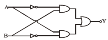
(a) OR gate
(b) XOR gate
(c) AND gate
(d) NAND gate
Answer: B
Question. The electrical conductivity of a semiconductor increases when electromagnetic radiation of wavelength shorter than 2480 nm is incident on it. The band gap (in eV) for the semiconductor is
(a) 0.9
(b) 0.7
(c) 0.5
(d) 1.1
Answer: C
Question. The diagram of a logic circuit is given below. The output F of the circuit is represented by
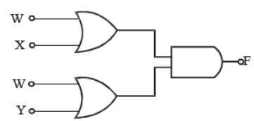
(a) W . (X + Y)
(b) W . (X . Y)
(c) W + (X . Y)
(d) W + (X + Y)
Answer: C
Question. In the half wave rectifier circuit operating from 50 Hz mains frequency, the fundamental frequency in the ripple would be
(a) 25 Hz
(b) 50 Hz
(c) 70.7 Hz
(d) 100 Hz
Answer: B
Question. A transistor is operated in common emitter configuration at VC = 2V such that a change in the base current from 100 mA to 300 mA produces a change in the collector current from 10mA to 20 mA. The current gain is
(a) 50
(b) 75
(c) 100
(d) 25
Answer: A
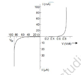
Question. In a p-n junction having depletion layer of thickness 10–6 m the potential across it is 0.1 V. The electric field is
(a) 107 V/m
(b) 10–6 V/m
(c) 105 V/m
(d) 10–5 V/m
Answer: C
Question. In the diagram, the input is across the terminals A and C and the output is across B and D. Then the output is
(a) zero
(b) same as the input
(c) full wave rectifier
(d) half wave rectifier
Answer: C
Question. A half-wave rectifier is being used to rectify an alternating voltage of frequency 50 Hz. The number of pulses of rectified current obtained in one second is
(a) 50
(b) 25
(c) 100
(d) 2000
Answer: B
Question. What is the conductivity of a semiconductor if electron density = 5 × 10¹²/cm3 and hole density = 8 × 10¹³/cm3 (μe = 2.3 m2 V–1 s–1, μh = 0.01 m2V–1 s–1)
(a) 5.634
(b) 1.968
(c) 3.421
(d) 8.964.
Answer: B
Question. The cause of the potential barrier in a p-n diode is
(a) depletion of positive charges near the junction
(b) concentration of positive charges near the junction
(c) depletion of negative charges near the junction
(d) concentration of positive and negative charges near the junction
Answer: D
Question. The ratio of electron and hole currents in a semiconductor is 7/4 and the ratio of drift velocities of electrons and holes is 5/4, then the ratio of concentrations of electrons and holes will be
(a) 5/7
(b) 7/5
(c) 25/49
(d) 49/25
Answer: B
Question. If A is the atomic mass number of an element, N is the Avogadro number and a is the lattice parameter, then the density of the element, if it has bcc crystal structure, is
(a) A/Na3
(b) 2A/Na3
(c) √3A/Na3
(d) 2√2A/Na3
Answer: B
Question. The current gain in transistor in common base mode is 0.99. To change the emitter current by 5 mA, the necessary change in collector will be
(a) 0.196 mA
(b) 2.45 mA
(c) 4.95 mA
(d) 5.1 mA
Answer: C
Question. In a reverse biased diode when the applied voltage changes by 1 V, the current is found to change by 0.5 μA. The reverse bias resistance of the diode is
(a) 2 × 10⁵ Ω
(b) 2 × 10⁶ Ω
(c) 200 Ω
(d) 2 Ω.
Answer: B
Question. The output of the given circuit in figure given below,
(a) would be zero at all times
(b) would be like a half wave rectifier with positive cycles in output
(c) would be like a half wave rectifier with negative cycles in output
(d) would be like that of a full wave rectifier
Answer: C
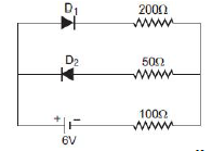
Question. In the circuit shown in figure given below, if the diode forward voltage drop is 0.3 V, the voltage difference between A and B is
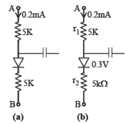
(a) 1.3 V
(b) 2.3 V
(c) 0
(d) 0.5 V
Answer: B
Question. The transistor are usually made of
(a) metal oxides with high temperature coefficient of resistivity
(b) metals with high temperature coefficient of resistivity
(c) metals with low temperature coefficient of resistivity
(d) semiconducting materials having low temperature coefficient of resistivity
Answer: A
Question. The truth table given below is for
(a) NOR
(b) AND
(c) XOR
(d) NAND
Answer: D
Question. In a full wave rectifier circuit operating from 50 Hz mains frequency, the fundamental frequency in the ripple would be
(a) 25 Hz
(b) 50 Hz
(c) 70.7 Hz
(d) 100 Hz
Answer: D
Question. The manifestation of band structure in solids is due to
(a) Bohr’s correspondence principle
(b) Pauli’s exclusion principle
(c) Heisenberg’s uncertainty principle
(d) Boltzmann’s law
Answer: B
Question. The frequency response curve of RC coupled amplifier is shown in figure. The band with of the amplifier will be (35 ex 2)
(a) f3 – f2
(b) f4 – f1
(c) f4 – f2/2
(d) f3 – f1
Answer: B
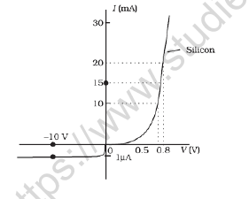
Question. A diode having potential difference 0.5 V across its junction which does not depend on current, is connected in series with resistance of 20Ω across source. If 0.1 A current passes through resistance then what is the voltage of the source?
(a) 1.5 V
(b) 2.0 V
(c) 2.5 V
(d) 5 V
Answer: C
Question. The difference in the variation of resistance with temperature in a metal and a semiconductor arises essentially due to the difference in the
(a) crystal structure
(b) variation of the number of charge carriers with temperature
(c) type of bonding
(d) variation of scattering mechanism with temperature
Answer: B
Question. Carbon, Silicon and Germanium atoms have four valence electrons each. Their valence and conduction bands are separated by energy band gaps represented by (Eg)C, (Eg)Si and (Eg)Ge respectively. Which one of the following relationship is true in their case?
(a) (Eg)C > (Eg)Si
(b) (Eg)C < (Eg)Si
(c) (Eg)C = (Eg)Si
(d) (Eg)C < (Eg)Ge
Answer: A
Please click on below link to download CBSE Class 12 Physics Semiconductor Materials Device And Simple Worksheet
| CBSE Class 12 Physics Semiconductor Materials Device And Simple Worksheet |
| CBSE Class 12 Physics Semiconductor Devices And Communication System Worksheet |
Free study material for Chapter 14 Semiconductor Electronics
Chapter 14 Semiconductor Electronics Materials Devices and Simple Circuits CBSE Class 12 Physics Worksheet
Students can use the Chapter 14 Semiconductor Electronics Materials Devices and Simple Circuits practice sheet provided above to prepare for their upcoming school tests. This solved questions and answers follow the latest CBSE syllabus for Class 12 Physics. You can easily download the PDF format and solve these questions every day to improve your marks. Our expert teachers have made these from the most important topics that are always asked in your exams to help you get more marks in exams.
NCERT Based Questions and Solutions for Chapter 14 Semiconductor Electronics Materials Devices and Simple Circuits
Our expert team has used the official NCERT book for Class 12 Physics to create this practice material for students. After solving the questions our teachers have also suggested to study the NCERT solutions which will help you to understand the best way to solve problems in Physics. You can get all this study material for free on studiestoday.com.
Extra Practice for Physics
To get the best results in Class 12, students should try the Physics MCQ Test for this chapter. We have also provided printable assignments for Class 12 Physics on our website. Regular practice will help you feel more confident and get higher marks in CBSE examinations.
You can download the teacher-verified PDF for CBSE Class 12 Physics Semiconductor Materials Device And Simple Worksheet from StudiesToday.com. These practice sheets for Class 12 Physics are designed as per the latest CBSE academic session.
Yes, our CBSE Class 12 Physics Semiconductor Materials Device And Simple Worksheet includes a variety of questions like Case-based studies, Assertion-Reasoning, and MCQs as per the 50% competency-based weightage in the latest curriculum for Class 12.
Yes, we have provided detailed solutions for CBSE Class 12 Physics Semiconductor Materials Device And Simple Worksheet to help Class 12 and follow the official CBSE marking scheme.
Daily practice with these Physics worksheets helps in identifying understanding gaps. It also improves question solving speed and ensures that Class 12 students get more marks in CBSE exams.
All our Class 12 Physics practice test papers and worksheets are available for free download in mobile-friendly PDF format. You can access CBSE Class 12 Physics Semiconductor Materials Device And Simple Worksheet without any registration.